상품상세정보
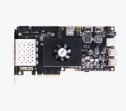
Xilinx Zynq-7000 FPGA Board
PCIe 2.0, SFP x4, Gigabit x 2 8GB EMMC, 2GB DDR3, HDMI Input/Output,GTX
Apply to PCIe, Video Image Proessing SFP / Ethernet Communicaion

Techinal Support
AX7Z100 Supporting Verilog HDL Demos and Docuemnts Linux Kernel: petalinux 4.9.0-xilinx-v2017.4 All Doucments Saved in Dropbox, after buy the board, email to get it.
Course_S1_Basic Tutorial
Part 1: Software Package Introduction and FPGA Board Inspection
Part 2: Introduction to ZYNQ
Part 3: Vivado development environment
Part 4: PL's "Hello World" LED experiment
Part 5: HDMI output experiment
Part 6: HDMI Pass-through ILA Debugging Experiment
Part 7: PL-side DDR3 read and write test
Part 8: GTX transceiver bit error rate test IBERT experiment
Part 9: Experience ARM, bare metal output "Hello World"
Part 10: PS lights up the LED lights of the PL
Part 11: PS timer interrupt experiment
Part 12: PL button interrupt experiment
Part 13:Ethernet Experiment (LWIP)
Part 14: Custom IP experiment
Part 15: Use VDMA to drive HDMI display
Part 16 Curing Programs
Part 17: PCIE Testing
Part 18: PCIe transmits video to HDMI display
Part 19: HDMI video input to PCIe capture display
Part 20: Developing PCIe under Linux
Part 21: Install virtual machine and Ubuntu system
Part 22: Ubuntu installs the Vivado software for Linux
Part 23: Petalinux tool installation
Part 24: NFS service software installation
Part 25: Customizing Linux with Petalinux
Part 26: Develop Linux programs using the SDK
Part 27: GPIO experiment under Linux
Part 28: HDMI display under Petalinux
Part 29: Use the Debian 8 desktop system
Part 30: Making QSPI Flash booted Linux
Part 31: QSPI and EMMC boot Linux输
Course_S2_SDK Application Tutorial
Part 1: PS side UART read and write control
Part 2: Use of XADC
Part 3: PL read and write PS DDR data
Part 4: Realize PS and PL data interaction through BRAM
Part 5: Use of dual core AMP
Part 6: Use of “Free RTOS”under ZYNQ
Part 7: DMA loop test
Part 8: Use of DMA--DAC waveform generator (AN108)
Part 9: Use of DMA--ADC oscilloscope (AN108)
Part 10: Use of DMA--ADC oscilloscope (AN926)
Part 11: Use of DMA--ADC oscilloscope (AN706)
Part 12: Use of the SG DMA based on ADC module (AN926)
Part 13: Use the SG DMA based on DAC module (AN9767)
Part 14: OV5640 camera acquisition display (1)
Part 15: OV5640 camera acquisition display (2)
Part 16: Binocular camera Ethernet transmission
Part 17: Use of 7 inch LCD module
Part 18: Use of 7-inch touch screen disaply
Part 19: SD card read and write operation BMP picture display
Part 20: SD card read and write operation camera capture
Part 21: Ethernet TransmissionADC Acquisition Based on AN926 Module
Part 22: Ethernet Transmission ADC Acquisition Based on AN706 Module
Part 23: Ethernet Transmission--ADC Acquisition Based on AN108 Module
Part 24: Remote update QSPI Flash based on UDP/TCP
Course_S3_HSL Application Tutorial
Part 1: Getting to Know HLS
Part 2: Status Indicator LED
Part 3: Floating Point Coprocessing
Part 4: Video Color Bar
Part 4: Realize PS and PL data interaction
Part 5: Video Frame Buffer Read and Write Management
Part 6: Image Scaling Overlay
Part 7: Character Overlay
Part 8: Image Contrast Adjustment
Part 9: Auto Focus
Part 10: Edge Detection
Part 11: Corner Detection
Part 12: Fast Fourier Transform
Course_S4_Linux Application Tutorial
Part 1: QT application on ZYNQ
Part 2: OpenCV Application (USB Camera Display)
Part 3: Binocular Camera Module OpenCV Display
Part 4: Touch screen module application
Part 5: AXI DMA Read and Write Test
Part 6: DMA-based ADC Waveform Display (AN926)
Part 7: DMA-based ADC Waveform Display (AN706)
Part 8: Autorun petalinux application
Part 9: Appendix - Linux Common Commands
Product Package
FPGA Board
AN9767 Collection Package
AN706 Collection Package
AN9238 Collection Package
Video Package
Luxury Package
FPGA Board
●
●
●
●
●
●
Downloader Cable USB
●
●
●
●
●
●
AN9767
●
●
AN706
●
●
AN9238
●
●
Binocular Camera
●
●
7-inch LCD
●
●
Supporting Modules in the Package, Click to Learn More


Key Features
·Core Board SOM


*Learn More about the Core Board, Click to View >
·FPGA Board

Product Parameters
Core Board Parameters
FPGA Board
AX7Z100
FPGA Chip
XC7Z100-2FFG900I
Kernel
Dual-Core ARM Cortex-A9 Main Frequency 800MHz
PL -end RAM
1GB DDR3 Data Rate 1600Mbps
PS -end RAM
1GB DDR3 Data Rate 1066Mbps
Speed Grades
-2
Chip Level
Industrial Grade
Working Temperature
-40°C~85°C
Logic Cells
444K
Look Up Tables (LUTs)
277400
CLB Flip-Flops
554800
Multiplier
2020
Transceivers
16-Channels Support PCIE Gen2 x 8
Block RAM
25.6Mbit
MIO
37
PL IO
162
Voltage Adjustable IO
96
LVDS
48 Pairs
Interface and Function
DDR3
32bit Bus, Data Rate 1066Mbps
QSPI Flash
512Mbit QSPI FLASH, Used as FPGA User Data Storage
EMMC Flash
8GB, Used as a Large-Capacity Storage Device in the ZYNQ System
Transceivers
16GTX,Each up to 6.25Gb/s, Used for SFP and PCIe Data Communication
SFP Interface
4-way High-Speed SFP Interface, the Receiving and Transmitting Speed of each Channel is up to 10.3125Gb/s
PCIe 2.0
AX7Z035 PCIe 2.0 x4, AX7Z100 PCIe 2.0 x8 Data Transmission Interface Single Channel Communication Rate up to 5GBaud
Ethernet Interface
Two 10/100M/1000M Ethernet RJ-45 Interfaces for Data Exchange
JTAG
Standard JTAG Port for Debug and Download of FPGA Program
HDMI
HDMI Video Input and Output Interface, up to 1080P@60Hz Support 3D Output and Data Input in Different Formats
USB 2.0 x 4
Used for Connect USB Peripherals such as Mouse, Keyboard.
USB Uart
Used for Serial Communication with PC or External Devices
Crystal Oscillator
33.333Mhz Provide Stable Clock Source for the PS System
200Mhz Provide DDR Reference Clock for the PL Logic
125Mhz Provide Reference Clock for the GTX Transceiver
Micro SD Card Slot
SD TF Card to Store Operating System Image and File System
LED
9 LEDs lights, 2 LEDs in the Core Board, 7 LEDs in the Carrier Board.
KEYs
5 Keys and 1 Reset Key, 4 PL User Keys
40-Pin Expansion Ports
Two 40-Pin Expansion Ports (0.1 inch Pitch), Can be Connect with Various ALINX Modules (Binocular Camera Module, TFT LCD Screen, Camera, AD/DA and Other Modules).
Power Supply Parameters
Voltage Input
+12 V DC
Current Input
Max. Current 2A
Package List
FPGA Board
1
USB Downloader Cable
1
Mini USB Cable
1
DC Fan (Fixed on the Board)
1
12V Power Adapter
1
Card Reader
1
TF Card
1
PCIe Fence
1
Structure Size
Size Dimension
Core Board 3.15 inch x 2.36 inch, Carrier Board 9.25 inch x 4.33 inch
Number of Layers
12-Layer Core Board PCB, 4-Layer Carrier Board PCB

Data Transmission Processing
4 High-Speed SFP Interfaces
Industrial Ethernet, Video Transmission Gigabit Ethernet and SFP Communication High-Speed Data Transmission Exchange
Optical Fiber Test Eye Diagram Each Optical Fiber Data Communication is up to 10Gb/s

Support PCIe 2.0 Standard
PCIE High-Speed Data Transmission
Meet PCIe Data Transmission and Video Image Processing

PCIe 2.0 x4 Read and write test

HDMI Video Input to PCIe Capture Display
Industrial Grade Core Board
Working Temperature -40℃ to 80℃
PASS High and Low Temperature Test

Binocular Camera Module Collection
Video Image Processing and Recognition
Security, Video Image Collection and Transmission Data Processing, Face Detection

7-inch Capacitive Screen Module
Touch Capacitive Screen UGUI
Develop and Manage the System Interface

Data Collection Display
Signal Data Acquisition System
AN9767/AN706 Module On-Board Demo

*The Signal Source Output Signal is Connected to the AN9767 Module, and the Waveform Signal is Displayed through the Oscilloscope
*The Signal Source Output Signal is Connected to the AN706 Module, Run the System to Draw the Waveform Data, and is Displayed to the Monitor through the HDMI Interface of the FPGA Development Board
배송안내
● 결제일로부터 1~3주 안에 배송됩니다.
● 제조사 재고가 부족하여 3주 안에 배송이 어려울 경우 메일로 안내해 드리니 참고하시기 바랍니다.
교환 및 반품안내
● 본 상품은 해외 재고 상품으로 기본적으로 교환 및 반품 처리가 어렵습니다.
● 상품에 따라 교환 및 반품 처리가 가능한 경우 비용이 수반되며 이니프로 고객센터에 연락하여 처리하시기 바랍니다.
환불안내
● 본 상품은 해외 재고 상품으로 기본적으로 환불 처리가 어렵습니다.
● 상품에 따라 환불이 가능한 경우 비용이 수반되며 이니프로 고객센터에 연락하여 처리하시기 바랍니다.
AS안내
● 제조사별로 A/S정책이 상이하니 하단 고객센터로 문의 주시기 바랍니다.
이미지 확대보기AX7Z100B


비밀번호 인증
글 작성시 설정한 비밀번호를 입력해 주세요.
장바구니 담기
상품이 장바구니에 담겼습니다.
바로 확인하시겠습니까?
찜 리스트 담기
상품이 찜 리스트에 담겼습니다.
바로 확인하시겠습니까?
CS CENTER
02-6956-9010문의 및 요청 사항을 1:1 문의 게시판에 남겨주시거나 sales@inipro.net 으로 메일을 보내주시면 최대한 빨리 처리해 드리도록 하겠습니다.
BANK INFO
1005-702-341569우리은행
예금주 : 이니프로주식회사