상품상세정보
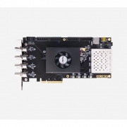
Professional SDI Procesor PCIE Development Platform
High Definition 3G-SDI Input Output Interfaces ,PCIE 2.0 X8· SFP Fiber Interface x4
Meet the requirements of users for various PCIe high-speed data transmission, video image processing and industrial control

Meet the requirements of users for various PCIe high-speed data transmission, video image processing and industrial control
技术支持
AV7K300 Supporting Verilog HDL Demos and Docuemnts.All Doucments Saved in Dropbox, after buy the board, email to get it.
00. vivado2017.4 Installation
01. LED water lamp experiment and simulation in vivado
02. Key detection experiment in Vivado
03. PLL Experiment in Vivado
04. Serial port Transmitting and Receiving experiment
05. Key debounce experiment
06. LM75 Temperature Test Experiment
07. SD Card Read and Write Experiment
08. SDI_LCD Test Experiment
09. DDR3 Read Write and Simulation Experiment
10. Recording and playback Experiment of AN831 Module
11. SD Card Music Player Experiment
12. Character Display Experiment
13. SD Card Read BMP Picture Display Experiment
14. OV5640 Camera Display Experiment
15. SOBEL Edge Detection Experiment
16. AD7606 Waveform Display Experiment
17. ADDA Testing Experiment
18. AD9767 Waveform Display Experiment-Dual channel Sine Wave Experiment
19. AD9767 Waveform Display Experiment-Dual channel Triangle Wave Experiment
20. GTX Fiber Optic Communication IBERT Testing Experiment
21. GTX Fiber Optic Data Communication Experiment
22. Video Image GTX Fiber Optic Communication Testing Experiment
23. PCIe Speed Test Experiment
24. PCIe SDI Input Experiment
25. PCIe SDI Output Experiment
26. PCIe xdma Interface Experiment Testing Experiment
Product Package
FPGA Board
AN9767 Collection Package
AN706 Collection Package
AN9238 Collection Package
Video Package
Luxury Package
FPGA Board
●
●
●
●
●
●
Downloader Cable USB
●
●
●
●
●
●
AN9767
●
●
AN706
●
●
AN9238
●
●
Binocular Camera
●
●
4.3-inch LCD
●
●
FPGA Board
AN9767 Collection Package
AN706 Collection Package
AN9238 Collection Package
Video Package
Luxury Package
FPGA Board
●
●
●
●
●
●
Downloader Cable USB
●
●
●
●
●
●
AN9767
●
●
AN706
●
●
AN9238
●
●
Binocular Camera
●
●
4.3-inch LCD
●
●
Supporting Modules in the Package, Click to Learn More


Key Features
·Core Board SOM


*Learn More about the Core Board, Click to View >
·FPGA Board

Product Parameters
Main Parameters
FPGA Chip
XC7K325T-2FFG900I
PCIe Gen2
X8
Logic Cells
326,080
Transceiver
16X 12.5Gb/s max
Look Up Tables (LUTs)
50,950
CLB Flip-Flops
407,600
Block RAM
16,020Kb
DSP
840
Temperature class
Industrial Grade, -40℃-85℃
XADC
1 个 12bit 1Mbps AD
Speed Grades
-2
FPGA Chip
XC7K325T-2FFG900I
PCIe Gen2
X8
Logic Cells
326,080
Transceiver
16X 12.5Gb/s max
Look Up Tables (LUTs)
50,950
CLB Flip-Flops
407,600
Block RAM
16,020Kb
DSP
840
Temperature class
Industrial Grade, -40℃-85℃
XADC
1 个 12bit 1Mbps AD
Speed Grades
-2
Interface and Function
DDR3
4 x 512MB DDR3, 64 bit Bus, Data Rate 1600Mbps
QSPI Flash
128Mbit, Used as FPGA User Data Storage
Crystal Oscillator
200MHz Provide Stable Clock Source for the System
125MHz Provide Stable Clock Source Input for the GTX transceiver
PCIe 2.0 x 8
Used for PCIe communication with computer motherboard Single Channel Communication Rate can be up to 5Gbps
SFP
4 SFP Interfaces, the Speed of Each Channel is up to 10Gb/s
JTAG
Standard JTAG Port for Debug and Download of FPGA Program
3G-SDI
HD 3G-SDI Interfaces, Support Data Input /Output in Different Formats ( HDcctv 1.0, HD-SDI(ST 292), 3G_SDI(ST-424) and SD_SDI(ST259)
JTAG
Standard JTAG Port for Debug and Download of FPGA Program
USB Uart
Used for Serial Communication with PC or External Devices
SD Card Slot
1Micro SD Card Slot, Support the SD Mode and SPI Mode
LED
4 User LEDs
Key
4 User Keys
40-Pin Expansion Ports
Reserved 40-Pin Expansion Ports (0.1 inch Pitch), Can be Connect with Various ALINX Modules (Binocular Camera Module, TFT LCD Screen, Camera, AD/DA and Other Modules).
Power Supply Parameters
Voltage Input
+12 V DC
Current Input
Max. Current 3A
Voltage Input
+12 V DC
Current Input
Max. Current 3A
Package List
FPGA Board
1
DC Fan (Fixed on the Board)
1
Mini USB Cable
1
USB Downloader Cable
1
12V Power Adapter
1
PCIe Fence
1
FPGA Board
1
DC Fan (Fixed on the Board)
1
Mini USB Cable
1
USB Downloader Cable
1
12V Power Adapter
1
PCIe Fence
1
Structure Size
Size Dimension
Core Board 3.15 inch x 2.36 inch, Carrier Board 8.46 inch x 4.37 inch
Number of Layers
8-Layer Core Board PCB, 6-Layer Carrier Board PCB Reserve Independent Power Layer and GND Layer

Core Board Size Dimension

Carrier Board Size Dimension
Size Dimension
Core Board 3.15 inch x 2.36 inch, Carrier Board 8.46 inch x 4.37 inch
Number of Layers
8-Layer Core Board PCB, 6-Layer Carrier Board PCB Reserve Independent Power Layer and GND Layer
Core Board Size Dimension
Carrier Board Size Dimension
Rich expansion interface
High-Speed Transmisson
SFP Communication, PCIe Aaccelerator Video Processing, High-Data Transmission

Core Board + Carrier Board, Customers Can Directly Use the Core Board in their Design.
Rich Interfaces in the Carrier board. PCIe x8 , 4 SFP, USB Uart, SD Card Slot 2 X 3G-SDI Output, Supports 1080P@60Hz Output 2 x 3G-SDI Input, Support 1080P@60Hz Input Apply to SDI Video Image Processing
SFP Communication, PCIe Aaccelerator Video Processing, High-Data Transmission
Core Board + Carrier Board, Customers Can Directly Use the Core Board in their Design.
Rich Interfaces in the Carrier board. PCIe x8 , 4 SFP, USB Uart, SD Card Slot 2 X 3G-SDI Output, Supports 1080P@60Hz Output 2 x 3G-SDI Input, Support 1080P@60Hz Input Apply to SDI Video Image Processing
High-speed optical fiber transmission
SFP Video Transmission and Speed
Binocular Camera Moulde for SFP Video Transmission


The FPGA Development Board Collects the Video Image through the Camera Module, Transmits it to Another FPGA Development Board through SPF, and displays to the PC Monitor through the SDI interface.

SFP 10G Transceiver Communication Eye Diagram
Binocular Camera Moulde for SFP Video Transmission
The FPGA Development Board Collects the Video Image through the Camera Module, Transmits it to Another FPGA Development Board through SPF, and displays to the PC Monitor through the SDI interface.
SFP 10G Transceiver Communication Eye Diagram
SDI Input and output
PCIE Data Acceleration Verification and Development
Verify PCIE Solution Speed up PCIE Product Development

Collect the Video Signal through the SDI Input Interface Upload it to the Computer Through the PCIE Interface, and Display the Video Image in Real Time

The Host Computer Grabs the Computer Desktop, and Transmits it to the FPGA through the PCIE Interface. The FPGA Outputs through the SDI Interface, The Monitor Displays in Real Time
Verify PCIE Solution Speed up PCIE Product Development
Collect the Video Signal through the SDI Input Interface Upload it to the Computer Through the PCIE Interface, and Display the Video Image in Real Time
The Host Computer Grabs the Computer Desktop, and Transmits it to the FPGA through the PCIE Interface. The FPGA Outputs through the SDI Interface, The Monitor Displays in Real Time
PCIE Read and Write
PCIE High-Speed Data Transmission
Meet various PCIe high-speed data transmission and video image processing

Meet various PCIe high-speed data transmission and video image processing
Binocular Camera Module
Camera Acquisition System
Dual Lens Camera Module On-Board Demo

Binocular Camera Module AN5642 for Video Capture Display on the Monitor through the SDI interface to Realize Binocular Display Simultaneously
Dual Lens Camera Module On-Board Demo
Binocular Camera Module AN5642 for Video Capture Display on the Monitor through the SDI interface to Realize Binocular Display Simultaneously
Data Collection Display
Signal Data Acquisition System
AN9767/AN706 Module On-Board Demo

*The Signal Source Output Signal is Connected to the AN9767 Module, and the Waveform Signal is Displayed through the Oscilloscope
*The Signal Source Output Signal is Connected to the AN706 Module Run the System to Draw the Waveform Data, and is Displayed to the Monitor through the SDI Interface of the FPGA Development Board
AN9767/AN706 Module On-Board Demo
*The Signal Source Output Signal is Connected to the AN9767 Module, and the Waveform Signal is Displayed through the Oscilloscope
*The Signal Source Output Signal is Connected to the AN706 Module Run the System to Draw the Waveform Data, and is Displayed to the Monitor through the SDI Interface of the FPGA Development Board
배송안내
● 결제일로부터 1~3주 안에 배송됩니다.
● 제조사 재고가 부족하여 3주 안에 배송이 어려울 경우 메일로 안내해 드리니 참고하시기 바랍니다.
교환 및 반품안내
● 본 상품은 해외 재고 상품으로 기본적으로 교환 및 반품 처리가 어렵습니다.
● 상품에 따라 교환 및 반품 처리가 가능한 경우 비용이 수반되며 이니프로 고객센터에 연락하여 처리하시기 바랍니다.
환불안내
● 본 상품은 해외 재고 상품으로 기본적으로 환불 처리가 어렵습니다.
● 상품에 따라 환불이 가능한 경우 비용이 수반되며 이니프로 고객센터에 연락하여 처리하시기 바랍니다.
AS안내
● 제조사별로 A/S정책이 상이하니 하단 고객센터로 문의 주시기 바랍니다.
이미지 확대보기AV7K300


비밀번호 인증
글 작성시 설정한 비밀번호를 입력해 주세요.
장바구니 담기
상품이 장바구니에 담겼습니다.
바로 확인하시겠습니까?
찜 리스트 담기
상품이 찜 리스트에 담겼습니다.
바로 확인하시겠습니까?
CS CENTER
02-6956-9010문의 및 요청 사항을 1:1 문의 게시판에 남겨주시거나 sales@inipro.net 으로 메일을 보내주시면 최대한 빨리 처리해 드리도록 하겠습니다.
BANK INFO
1005-702-341569우리은행
예금주 : 이니프로주식회사