상품상세정보
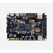
Xilinx Spartan-7 FPGA Development Board
1G DDR3, QSPI Flash, Gigabit Ethernet, USB, HDMI,RTC
Data Transmission, Video Image Processing and Industrial Control Gigabit Ethernet and USB Communication Pre-validation and Post-application of Data Processing

Data Transmission, Video Image Processing and Industrial Control Gigabit Ethernet and USB Communication Pre-validation and Post-application of Data Processing
Techinal Support
AX7050 Supporting Verilog HDL Demos and Docuemnts,All Doucments Saved in Dropbox, after buy the board, email to get it.
00.vivado2019.1 Installation
01.LED water lamp experiment and simulation in vivado
02. Key detection experiment in Vivado
03.PLL Experiment in Vivado
04.Serial port Transmitting and Receiving experiment
05.Key debounce experiment
06.I2C Interface EEPROM Experiment
07.FPGA on-chip ROM read and write Experiment
08.FPGA on-chip RAM read and write Experiment
09.FPGA on-chip FIFO read and write Experiment
10.SD Card Read and Write Experiment
11.HDMI Programming Output Experiment
12.DDR3 Read Write and Simulation Experiment
13.Recording and playback Experiment of AN831 Module
14.SD Card Music Player Experiment
15.Character Display Experiment
16.SD Card Read BMP Picture Display Experiment
17.OV5640 Camera Display Experiment
18.SOBEL Edge Detection Experiment
19.AD9238 Waveform Dispaly Experiment
20.AD7606 Waveform Display Experiment
21.ADDA Testing Experiment
22.AD9767 Waveform Display Experiment-Dual channel Sine Wave Experiment
23.AD9767 Waveform Display Experiment-Dual channel Triangle Wave Experiment
24.Ds1302 Digital Tube Display RTC Time Experiment
25.Gigabit Ethernet transmission experiment
26.AD9238 Chip Ethernet Transmission
27.AD7606 Chip Ethernet Transmission Experiment
28.AD9280 Chip Ethernet Communication
29.Gigabit Ethernet Video Transmission Experiment
30.USB Two-way Speed Measurement Experiment
Product Package
AN108 AD/DA Collection Package
AN9767 DA Collection Package
AN706 AD Collection Package
AN9238 AD Collection Package
AN5642 Binocular Camera Package
Monocular Camer Video Package
Luxury Package
FPGA Board
●
●
●
●
●
●
●
USB Downloader
●
●
●
●
●
●
●
AN108
●
●
AN9767
●
●
AN706
●
●
AN9238
●
●
AN5642
●
●
AN5640
●
●
AN430 4.3-Inch LCD
●
●
Supporting Modules in the Package, Click to Learn More


key Features
·Core Board SOM


*Core Board AC7050, Click to Purchase>
·FPGA Board

PRODUCT PARAMETERS
FPGA Chip Parameters
FPGA Chip
XC7S50-1FGGA484I
DDR3
1GB,数据频率333.3MHz
Logic Cells
52160
Look Up Tables (LUTs)
8150
Number of Expansion IOs
114
LVDS Differential Pair
37
Speed Grades
-1
CLB Flip-Flops
65200
DSP
120个
Block RAM
2700Kb
Adjustable Voltage IO
75 IOs
Speed Grades
Industrial Grade
Working Temperature
-40°C to 85°C
Interface and Function
DDR3
1GB DDR3 32bit, Data Rate 667Mbps
QSPI Flash
128Mb, Used as Storage for FPGA Configuration Files and User Data
Gigabit Ethernet
10/100/1000M Ethernet with RJ-45 Interface for Ethernet Data Exchange
USB Uart
Used for Serial Communication with PC or External Devices
USB 2.0
Used for USB 2.0 High Speed Communication with PC
HDMI Output
Support Different Format Video Output.
Camera Interface
Connected with 5 million OV5640 Monocular Camera Module AN5640
JTAG
10-pin 0.1-inch Standard JTAG Port for Programs Debug and Download
Real Time Clock
RTC with a Battery Holder, The Battery Model is CR1220
EEPROM
EEPROM 24LC04 with IIC Interface On-Board
40-Pin Expansion Ports
One 40-Pin Expansion Ports (0.1 inch Pitch), Can be Connect with Various ALINX Modules (Binocular Camera Module, TFT LCD Screen, Camera, AD/DA and Other Modules).
LED
5 User LEDs(1 LED in Core Board, 4 LEDs in the Carrier Board)
KEYs
4 User KEYs
Crystal Oscillator
50MHz Provide Stable Clock Source for the System
SD Card Slot
1 Micro SD Card Slot, Support SD Mode and SPI Mode
Power Supply Parameters
Voltage Input
+5 V DC
Current Input
Max. Current 2A
Voltage Input
+5 V DC
Current Input
Max. Current 2A
Package List
FPGA Board
1
USB Downloader Cable
1 Set
Mini USB Cable
1
Transparent Protection Board
1
5V Power Adapter
1
FPGA Board
1
USB Downloader Cable
1 Set
Mini USB Cable
1
Transparent Protection Board
1
5V Power Adapter
1
Structure Size
Size Dimension
Core Board 2.17 inch x 1.77 inch, Carrier Board 5.12 inch x 3.54 inch
Number of Layers
8-Layer Core Board PCB, 4-Layer Carrier Board PCB

Size Dimension
Core Board 2.17 inch x 1.77 inch, Carrier Board 5.12 inch x 3.54 inch
Number of Layers
8-Layer Core Board PCB, 4-Layer Carrier Board PCB
USB data transfer demo
USB 2.0 Communication Interface
FT232H Driver Chip for USB Data Transmission up to 45MB/s

FT232H Driver Chip for USB Data Transmission up to 45MB/s
Video capture demo
Camera Acquisition System
Video Capture, Remote Control, Picture Processing

The Monocular Camera Module AN5640 for Video Capture, and Displays it on the Monitor through the HDMI Interface

The Monocular Camera Module for SOBEL Edge Detection, and Displays it on the Monitor through the HDMI Interface

The Binocular Camera Module AN5642 for Video Capture, and Displays it on the Monitor through the HDMI Interface
Video Capture, Remote Control, Picture Processing
The Monocular Camera Module AN5640 for Video Capture, and Displays it on the Monitor through the HDMI Interface
The Monocular Camera Module for SOBEL Edge Detection, and Displays it on the Monitor through the HDMI Interface
The Binocular Camera Module AN5642 for Video Capture, and Displays it on the Monitor through the HDMI Interface
Data Collection Display
Signal Data Acquisition System
AN9767/AN706 Module On-Board Demo

* The Signal Source Output Signal is Connected to the AN9767 Module, and the Waveform Signal is Displayed through the Oscilloscope
* The Signal Source Output Signal is Connected to the AN706 Module, Run the System to Draw the Waveform Data, and is Displayed to the Monitor through the VGA Interface of the FPGA Development Board
AN9767/AN706 Module On-Board Demo
* The Signal Source Output Signal is Connected to the AN9767 Module, and the Waveform Signal is Displayed through the Oscilloscope
* The Signal Source Output Signal is Connected to the AN706 Module, Run the System to Draw the Waveform Data, and is Displayed to the Monitor through the VGA Interface of the FPGA Development Board
배송안내
● 결제일로부터 1~3주 안에 배송됩니다.
● 제조사 재고가 부족하여 3주 안에 배송이 어려울 경우 메일로 안내해 드리니 참고하시기 바랍니다.
교환 및 반품안내
● 본 상품은 해외 재고 상품으로 기본적으로 교환 및 반품 처리가 어렵습니다.
● 상품에 따라 교환 및 반품 처리가 가능한 경우 비용이 수반되며 이니프로 고객센터에 연락하여 처리하시기 바랍니다.
환불안내
● 본 상품은 해외 재고 상품으로 기본적으로 환불 처리가 어렵습니다.
● 상품에 따라 환불이 가능한 경우 비용이 수반되며 이니프로 고객센터에 연락하여 처리하시기 바랍니다.
AS안내
● 제조사별로 A/S정책이 상이하니 하단 고객센터로 문의 주시기 바랍니다.
이미지 확대보기AX7050


비밀번호 인증
글 작성시 설정한 비밀번호를 입력해 주세요.
장바구니 담기
상품이 장바구니에 담겼습니다.
바로 확인하시겠습니까?
찜 리스트 담기
상품이 찜 리스트에 담겼습니다.
바로 확인하시겠습니까?
CS CENTER
02-6956-9010문의 및 요청 사항을 1:1 문의 게시판에 남겨주시거나 sales@inipro.net 으로 메일을 보내주시면 최대한 빨리 처리해 드리도록 하겠습니다.
BANK INFO
1005-702-341569우리은행
예금주 : 이니프로주식회사