상품상세정보
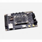
China PANGOMICRO Logos2 FPGA SoM Core Board
HDMI output interface, USB, Ethernet, camera interface, JTAG debugging interface, 1-way 40PIN extension port, RTC clock, etc. meet the requirements of video image processing and industrial control

Techinal Support
Supporting Verilog HDL Demos and Docuemnts,All Doucments Saved in Dropbox, after buy the board, email to get it.
01. Pango Design Suite 2021.1-sp7 Installation
02. LED water lamp experiment and simulation
03. Key detection experiment
04. PLL phase-locked loop output test
05. Serial port Transmitting and Receiving experiment
06. Key debounce experiment
07. I2C Interface EEPROM Experiment
08. SD Card Read and Write Experiment
09. HDMI Programming Output Experiment
10. 4.3 inch screen color bar output
11. 7-inch screen color bar output
12. SDRAM read and write data testing
13. AN831 Recording and Playback
14. SD Card Music Player Experiment
15. Character HDMI display
16. Character 4.3 inch screen display
17. Character 7-inch screen display
18. SD card image HDMI display
19. SD card image 4.3 inch LCD display
20. SD card image displayed on a 7-inch screen
21. AN5640 camera captures HDMI display
22. AN5640 camera captures a 4.3 inch screen display
23. AN5640 camera captures 7-inch screen display
24. AN5642 binocular camera captures HDMI display
25. Camera edge detection HDMI display routine
26. Camera edge detection 4.3 inch screen display routine
27. Camera edge detection 7-inch screen display routine
28. AD9238 waveform display routine
29. AD7606 waveform display routine
30. ADDA Test Routine
31. AD9767 Dual Channel Sine Wave Generation Routine
32. AD9767 Dual Channel Triangular Wave Generation Routine
33. RTC Clock Experiment
34. Gigabit Ethernet Transmission Experiment
35. AD 9280 Ethernet transmission routine
36. AD7606 Ethernet Transmission Routine
37. AD9280 Ethernet Transmission Routine
38. AN5640 Gigabit Ethernet for video transmission
39. AN5642 Gigabit Ethernet for video transmission
40. USB bidirectional speed measurement routine
Product Package
AN108 Collection Package
AN9767Collection Package
AN706 Collection Package
AN9238 Collection Package
Binocular Camera Package
Single camera video package
Luxury Package
FPGA Board
●
●
●
●
●
●
●
USB Downloader
●
●
●
●
●
●
●
AN108
●
●
AN9767
●
●
AN706
●
●
AN9238
●
●
AN5642
●
●
AN5640
●
●
4.3-Inch LCD
●
●
Supporting Modules in the Package, Click to Learn More


Key Features
·Core board


Learn More about the Core Board, Click to View>>
·FPGA Board

Product Parameters
SoM Core Board Parameters
FPGA Chip
PGL50H-6IFBG484
Chip level
Chip speed level -6, chip temperature level industrial grade
Flip-Flop ( FF )
64200
LUT5
42800 ( LUT5=1.2LUT4 )
DRM ( 18Kbits )
134
APM Unit ( Multiplier )
84
PCIe Gen2 x4
1
HSST
4x 6.375Gb/s max
PLL
5
AES
1
Interface and Function
DDR3
2x 512MB, 1GB in total, 32bit bus for data caching
QSPI Flash
128Mbit QSPI FLASH, Used for FPGA Configuration File and User Data Storage
Crystal Oscillator
1x 125MHz active differential crystal oscillator, providing reference input clock for the internal HSST module of FPGA
50 Mhz Provide Reference Input Clock for FPGA
HDMI Output
1 channel HDMI output, providing video output interfaces in different formats for the development board
Gigabit Ethernet
One 10 / 100M / 1000M Ethernet with RJ-45 Interfaces for Data Exchange
USB
1-way USB2.0 interface for high-speed communication between development board and PC using USB2.0
Uart
1-way Uart to USB interface for communication with computers, facilitating user debugging
EEPROM
1 EEPROM 24LC04 with IIC interface
CMOS
18-pin camera interface that can connect to a 5 million OV5640 camera
RTC
One way RTC Real-time clock, equipped with battery holder, and the battery model is CR1220 (self purchased)
JTAG
10-pin 2.54mm standard JTAG port for downloading and debugging FPGA programs
SD Card Slot
1 Micro SD Card Slot, Support the SPI Mode
LED
5 User LEDs (1 LED in the Core Board, 4 LEDs in the Carrier Board )
KEYs
4
40-Pin Expansion Ports
1x 40-pin 2.54mm spacing expansion port, capable of connecting various modules ( binocular camera, LCD screen, high-speed AD module, etc ) The expansion port includes 1x 5V power supply, 2x 3.3V power supplies, 3 ground supplies, and 34 IO ports
Power Supply Parameters
power supply
5V, 2A
Package List
FPGA Board
1
USB Downloader Cable
1 Set
Mini USB Cable
1
5V power supply
1
12V Power Adapter
1
Structure Size
Size Dimension
130mm x 90mm
Number of Layers
14-Layer Core Board PCB, 4-Layer Carrier Board PCB


PANGOMICRO
FPGA China Solution

The Logos series FPGA adopts a 40nm CMOS process and a new LUT5 structure, integrating rich on-chip resources such as RAM, DSP, ADC, Serdes, DDR3, and IO interfaces. It has low power consumption, low cost, and rich functions, providing customers with cost-effective solutions. It is widely used in industrial control, communication, consumer fields, and other fields, making it an ideal choice for customers in large-scale, cost sensitive projects.
Binocular collection Display
Video Transmission Processing

The Binocular Camera Module AN5642 for Video Capture Displays it on the Monitor through the HDMI Interface and Realize Binocular Display Simultaneously
Data Collection Display
Signal Data Acquisition System
AN9767 / AN706 Module On-Board Demo

*The Signal Source Output Signal is Connected to the AN9767 Module, and the Waveform Signal is Displayed through the Oscilloscope
*The Signal Source Output Signal is Connected to the AN706 Module, Run the System to Draw the Waveform Data, and is Displayed to the Monitor through the HDMI Interface of the FPGA Development Board
Direct operation on the palm
4.3 Inch LCD Screen

배송안내
● 결제일로부터 1~3주 안에 배송됩니다.
● 제조사 재고가 부족하여 3주 안에 배송이 어려울 경우 메일로 안내해 드리니 참고하시기 바랍니다.
교환 및 반품안내
● 본 상품은 해외 재고 상품으로 기본적으로 교환 및 반품 처리가 어렵습니다.
● 상품에 따라 교환 및 반품 처리가 가능한 경우 비용이 수반되며 이니프로 고객센터에 연락하여 처리하시기 바랍니다.
환불안내
● 본 상품은 해외 재고 상품으로 기본적으로 환불 처리가 어렵습니다.
● 상품에 따라 환불이 가능한 경우 비용이 수반되며 이니프로 고객센터에 연락하여 처리하시기 바랍니다.
AS안내
● 제조사별로 A/S정책이 상이하니 하단 고객센터로 문의 주시기 바랍니다.
이미지 확대보기AXPGL50H


비밀번호 인증
글 작성시 설정한 비밀번호를 입력해 주세요.
장바구니 담기
상품이 장바구니에 담겼습니다.
바로 확인하시겠습니까?
찜 리스트 담기
상품이 찜 리스트에 담겼습니다.
바로 확인하시겠습니까?
CS CENTER
02-6956-9010문의 및 요청 사항을 1:1 문의 게시판에 남겨주시거나 sales@inipro.net 으로 메일을 보내주시면 최대한 빨리 처리해 드리도록 하겠습니다.
BANK INFO
1005-702-341569우리은행
예금주 : 이니프로주식회사