상품상세정보
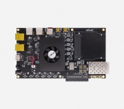
Xilinx Zynq 7000 FPGA Board
PCIe 2.0 x4 , SFP Module, Connector x2, Gigabit Ethernet x2, USB2.0 x 4, HDMI Output Interface x 1, FMC Interfacex1
Apply to Data Exchange and Storage, Video Transmission Optical Fiber/Ethernet Communication,Industrial Control

Apply to Data Exchange and Storage, Video Transmission Optical Fiber/Ethernet Communication,Industrial Control
Techinal Support
AX7350 Supporting Verilog HDL Demos and Docuemnts . All Doucments Saved in Dropbox, after buy the board, email to get it.
Part 01: FPGA Development Board AX7350 Introduction and Inspection
Part 02: Introduction to ZYNQ
Part 03: Vivado development environment
Part 04: PL's "Hello World" LED experiment
Part 05: HDMI output experiment
Part 06: Programmable clock SI5338 experiment
Part 07: PL end DDR3 read and write test
Part 08: GTX transceiver bit error rate test IBERT experiment
Part 09: Experience ARM, bare metal output "Hello World"
Part 10: PS lights up the LED lights of the PL
Part 11: PS timer interrupt experiment
Part 12: PL button interrupt experiment
Part 13: Ethernet Experiment (LWIP)
Part 14: Custom IP experiment
Part 15: Use VDMA to drive HDMI display
Part 16: Curing procedure
Part 17: PCIe ROOT Enumeration test
Part 18: Install virtual machine and Ubuntu system
Part 19: Ubuntu installs theVivado software for Linux
Part 20: Petalinux tool installation
Part 21: NFS service software installation
Part 22: Customizing Linux with Petalinux
Part 23: Develop Linux programs using the SDK
Part 24: GPIO experiment under Linux
Part 25: HDMI display under Petalinux
Part 26: Use the Debian 8 desktop system
Part 27: PCIe SSD application
Part 28: QSPI and EMMC boot Linux
Product Package
FPGA Board
HDMI Package
AD Packge
Camera Package
4 Ethernet Package
Luxury Package
FPGA Board
●
●
●
●
●
●
FL9134
●
●
FL9627
●
●
FL0214
●
●
FL9031
●
●
Supporting Modules in the Package, Click to Learn More


Key Features
·FPGA Board

RODUCT PARAMETERS
Main Parameters
FPGA Board
AX7350
FPGA Chip
XC7Z035-2FFG676I
Kernel
Dual-Core ARM Cortex-A9, Main Frequency 800MHz
PL -end RAM
1GB DDR3, Data Rate 1600Mbps
PS -end RAM
1GB DDR3, Data Rate 1066Mbps
GTX Transceivers
8 -Channels Support PCIE Gen2 x 8
Speed Grades
-2
Working Temperature
-40°C~85°C
Look Up Tables (LUTs)
171900
CLB Flip-Flops
343800
eMMC FLASH
8GB
MIO(ARM Side)
37
Voltage Adjustable IO
96
Chip Level
Industrial Grade
Logic Cells
275k
Multiplier
900(18x25MACCs)
Block RAM
17.6Mbit
QSPI FLASH
256MBit
PL IO(FPGA)
144
LVDS
48
Interface and Function
DDR3
DDR3 on the PS Side, 32bit Bus, can be Used as ZYNQ Chip Data Cache, Operating System Memory.
DDR3 on the PL Side,32bit bus, can be Used as FPGA Data Storage, Image Analysis Buffer Data Processing
QSPI Flash
256Mbit, Used as FPGA User Data Storage
EMMC Flash
8GB, Used as a Large-Capacity Storage Device in the ZYNQ System
SFP Interface
2-way High-Speed SFP Interface, the Receiving and Transmitting Speed of each Channel is up to 10.3125Gb/s
PCIe 2.0 x 8
Support PCIe 2.0 x4 ROOT Mode, Single Channel Communication Rate can be as be Up to 5GBaud, Can Connect to NVMe SSD
Ethernet Interface
2 10/100M/1000M Ethernet RJ-45 Interfaces for Data Exchange
JTAG
USB JTAG Debugging Interface, Used for TAG Interface to Debug and Download ZYNQ System
HDMI Output
HDMI Video Output Interface, Support up to 1080P@60Hz Output, Support 3D Output
USB Uart
Used for Serial Communication with PC or External Devices
USB 2.0 x 4
Used to Connect USB Peripherals such as Mouse and Keyboard
Crystal Oscillator
33.333Mhz Provide Stable Clock Source for the PS System
50MHz, Provide Extra Clock for PL Logic
Programmable ClockChip provide the Clock Source for GTX and a Reference Clock for PCIE, SFP and DDR operations
TF Card Slot
TF Card for Store Operating System Image and File System
LED
5 LEDs, 1 LED Controlled by PS, 4 LEDs Controlled by PL.
KEYs
6 KEYs, 1 Reset KEY, 1 KEY Controlled by PS and 4 KEYs Controlled by PL.
FMC Expansion Port
Standard FMC HPC Expansion PortCan be Connect with Various XILINX or ALINX FMC Modules (HDMI Input/Output Module, Binocular Camera Module, Hight Speed AD Module). FMC expansion port contains 84 pairs of differential IO signals and 8 high-speed GTX transceiver signals
Power Supply Parameters
Voltage Input
+12V DC
Current Input
Max. Current 2A
Voltage Input
+12V DC
Current Input
Max. Current 2A
Package List
FPGA Board
1
DC Fan (Fixed the Board)
1
Mini USB Cable
2
Transparent Protection Board
1
12V Power Adapter
1
Card Reader
1
TF Card
1
FPGA Board
1
DC Fan (Fixed the Board)
1
Mini USB Cable
2
Transparent Protection Board
1
12V Power Adapter
1
Card Reader
1
TF Card
1
Structure Size
Size Dimension
8.66 inch x 4.92 inch
Number of Layers
12-Layer PCB

Size Dimension
8.66 inch x 4.92 inch
Number of Layers
12-Layer PCB
Data Transmission Processing
2 High-Speed SFP Interfaces
Industrial Ethernet, Video Transmission Gigabit Ethernet and SFP Communication High-Speed Data Transmission Exchange

Industrial Ethernet, Video Transmission Gigabit Ethernet and SFP Communication High-Speed Data Transmission Exchange
High-Speed SFP Video Transmission
SFP Video Transmission Demo
FMC Camera Module FL0214 is Connected to FMC Inteface to realize optical fiber video transmission

The FPGA Development Board Collects Video Images through the Camera Module,and Transmits it to another FPGA Development Board through the SFP Interface. After the SFP Interface Receives the Data, Displayed it to the Monitor through the HDMI Interface.

SFP Transceiver Communication Eye Diagram
FMC Camera Module FL0214 is Connected to FMC Inteface to realize optical fiber video transmission
The FPGA Development Board Collects Video Images through the Camera Module,and Transmits it to another FPGA Development Board through the SFP Interface. After the SFP Interface Receives the Data, Displayed it to the Monitor through the HDMI Interface.
SFP Transceiver Communication Eye Diagram
Xilinx/Alinx FMC Module
Standard FMC HPC Interface
34 Pairs of Differential IO Signals 1 High-Speed GTX Transceiver Signals

34 Pairs of Differential IO Signals 1 High-Speed GTX Transceiver Signals
PCIe High-Speed Data Communication
PCIe 2.0 x4 Slot Interface
Single Channel Communication rate up to 5GBaud


Single Channel Communication rate up to 5GBaud
배송안내
● 결제일로부터 1~3주 안에 배송됩니다.
● 제조사 재고가 부족하여 3주 안에 배송이 어려울 경우 메일로 안내해 드리니 참고하시기 바랍니다.
교환 및 반품안내
● 본 상품은 해외 재고 상품으로 기본적으로 교환 및 반품 처리가 어렵습니다.
● 상품에 따라 교환 및 반품 처리가 가능한 경우 비용이 수반되며 이니프로 고객센터에 연락하여 처리하시기 바랍니다.
환불안내
● 본 상품은 해외 재고 상품으로 기본적으로 환불 처리가 어렵습니다.
● 상품에 따라 환불이 가능한 경우 비용이 수반되며 이니프로 고객센터에 연락하여 처리하시기 바랍니다.
AS안내
● 제조사별로 A/S정책이 상이하니 하단 고객센터로 문의 주시기 바랍니다.
이미지 확대보기AX7350B


비밀번호 인증
글 작성시 설정한 비밀번호를 입력해 주세요.
장바구니 담기
상품이 장바구니에 담겼습니다.
바로 확인하시겠습니까?
찜 리스트 담기
상품이 찜 리스트에 담겼습니다.
바로 확인하시겠습니까?
CS CENTER
02-6956-9010문의 및 요청 사항을 1:1 문의 게시판에 남겨주시거나 sales@inipro.net 으로 메일을 보내주시면 최대한 빨리 처리해 드리도록 하겠습니다.
BANK INFO
1005-702-341569우리은행
예금주 : 이니프로주식회사